

Highlight
Cameras that count photons
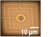
Single-photon avalanche diode
Achievement/Results
Fluorescence lifetime imaging microscopy is a powerful imaging technique that exploits the sensitivity of a fluorescent dye’s lifetime to its chemical and physical environment. In addition, the proximity of secondary dyes can influence the fluorescence lifetime through fluorescence resonance energy transfer (FRET). The most common measurement system for FLIM uses photomultiplier tubes (PMTs) or discrete single photon avalanche diodes (SPADs) in Geiger mode to perform time-correlated single-photon counting (TCSPC). In TCSPC the fluorophore is excited with a short laser pulse and the arrival time of the first photon to register a hit on the detector is recorded through time-to-digital conversion (TDC). Traditionally this modality requires tens of seconds to record a histogram of arrival times that is sufficient for extracting the fluorescence lifetime at each pixel from which an image can be formed. Recently, there have been efforts to integrate SPADs into CMOS processes to create arrays that would allow for higher frame rates through wide-field imaging. However, these devices are still limited to only a few frames per second. The focus of this research is to combine statistical analysis with tailored hardware to develop an imaging device that is capable of performing FLIM at frame rates exceeding 100 Hz. Such frame rates will open new application areas for FLIM.
In order to develop such an imager, we first needed to integrate SPADs in a relatively modern CMOS process. We chose the 130-nm CMOS node because it offers fast circuit devices (Fanout of 4 of less than 40 ps) and transistor diffusion implants that could be repurposed to create a SPAD with peak sensitivity around 500 nm. More advanced CMOS processes use higher dopant concentrations for the source and drain implants of the transistors that, if repurposed for a photosensitive device, would shift the peak sensitivity to shorter wavelengths. The detection limits of SPADs are determined by the device’s noise in the form of its dark count rate (DCR). DCR is typically dominated by thermal generation of carriers from recombination-generation (RG) centers close to the multiplication region of the SPAD, which triggers a false avalanche event. At technology nodes below 0.35 µm, the shallow trench isolation that is used to separate devices creates a defect-rich interface that is a significant source of RG centers. In our SPAD design, we isolated the STI interfaces from the multiplication region by repurposing the standard design masks of an established 130-nm CMOS process. In order to compare the performance of our SPAD design to those made in other CMOS processes, we developed a FLIM-specific figure of merit that is based on the probabilities associated with the Poisson statistics that describe fluorescence decay. We were able to develop a device that is one of the best performing at the 130-nm node and is comparable to devices fabricated in LOCOS processes.
After successfully designing a SPAD in 130-nm technology, we designed a fully-integrated system to perform TCSPC that is optimized for FLIM. We designed a 64 × 64 pixel array of SPADs, each with independent time measurement circuitry and a custom data path that will enable accurate FLIM with frame rates in excess of 100 Hz. The TDCs for each pixel provide a timing resolution less than 70 ps with a maximum range of at least 64 ns, which provides the flexibility to measure fluorophores with lifetimes ranging from 2-20ns. The data path exploits some of the statistical analysis used for developing the SPAD figure-of-merit to create a FLIM specific path that efficiently packages the data for all pixels that register a photon event. This approach reduces the number of data storage elements required on chip and also lowers the bandwidth requirements for transmitting the data off chip without sacrificing accuracy. We have also designed banks of low-voltage differential signaling (LVDS) drivers for efficiently sending up to 42 Gbps of data from the chip to a receiving field programmable gate array (FPGA). This data path and transmission circuitry is made possible because of the fast devices that are available in the 130-nm process.
The custom IC will interface, through its LVDS drivers, with four FPGAs on a printed circuit board (PCB) These FPGAs will create histograms of the photon arrival times for each pixel in the image. By creating histograms at the PCB level, further compression of the data is achieved and the bandwidth requirement is reduced to less than 200 Mbps. This data rate can be transmitted to a standard personal computer over a USB interface and recorded to the hard drive in real time. The PCB is designed so that the imaging chip can be fitted in the standard camera port of an upright microscope.
With the development of this new high-speed imager, we have also been exploring applications that will exploit the high frame rate of the device. One such application in small animal imaging is FLIM of intrinsic fluorophores to monitor metabolism. The two coenzymes nicotinic adenine dinucleotide (NADH) and flavin adenine dinucleotide (FAD) are naturally fluorescent and have varying fluorescent lifetimes that depend on whether or not these molecules are free or protein bound. Whether the coenzyme is bound or unbound can be used to distinguish between cancerous and healthy cells. This high-speed FLIM array provides the capability to perform in vivo imaging that was not previously possible due to motion of the specimen during the long acquisition times. This imaging device has the potential to be translated to a clinical setting whereby, for example, endoscopic imaging based on these metabolic indicators could provide a real-time determination between cancerous and healthy tissue.
This work involved IGERT Associate Ryan Field, working with IGERT faculty, Profs. Shepard, Hillman, and Paninsky (electrical engineering, biomedical engineering, and statistics).
Address Goals
In this project, the combined efforts of researchers in electrical engineering, biomedical engineering, and statistics have led to the design of an imaging device that has the potential to transform the landscape of FLIM. By drastically decreasing the image acquisition time for this technique, we have created the opportunity to explore dynamic interactions using a form of contrast other than wavelength, as is commonly used in traditional camera imaging. The applications of this technique are sure to exceed those that we currently consider to be the most promising – in vivo imaging of intrinsic metabolic markers and dynamic binding events using FRET. The ability to perform real-time in vivo imaging of these metabolic markers could be a major advancement in the ability to quickly and accurately perform disease diagnosis.
At the completion of this research project, our high-speed FLIM device would be a good candidate for commercialization. The current state of the art in FLIM is thousands of times slower and costs hundreds of times more than our device. As such, we anticipate a great opportunity to provide the research community with a low-cost solution to FLIM that will outperform all other devices. Through reduced cost and improved performance, we hope to make FLIM ubiquitous. As it becomes more wide-spread, it is likely that new uses for FLIM will develop and further advances in scientific measurement can be made.
The graduate students that work on this project are required to collaborate with researchers in biology, biomedical engineering, electrical engineering, and statistics in order to understand all aspects of the problem being addressed. These interdisciplinary interactions lead to a well-rounded group of science and engineering students that can apply skills gained from this project to many other areas of research. For example, the mathematics used to describe the fluorescence decay can also be applied to neural spike train analysis and the ability to build integrated systems on a chip finds widespread application throughout the sciences. These students will be well equipped for careers in the rapidly evolving science and engineering research community.
The graduate student currently working on this project has co-developed two lectures on biological sensing and imaging to present as part of the Columbia University Science Honors Program (SHP). SHP is an academic enrichment program for motivated, high-performing high school students from New York City and the surrounding area. By sharing cutting-edge research with these students, we have directly helped to improve the scientific literacy of the next generation of top college students while also encouraging them to pursue further education in science and engineering. In addition, this graduate student has helped develop and present several project-based engineering education modules for use in high schools. These modules aim to present engineering principles while motivating students with hands-on learning. We presented these modules at Samuel Gompers High School in Bronx, NY to a pre-engineering class.
