

Highlight Photo
Silicon FinFET devices as terahertz detectors
Silicon FinFET devices as terahertz detectors
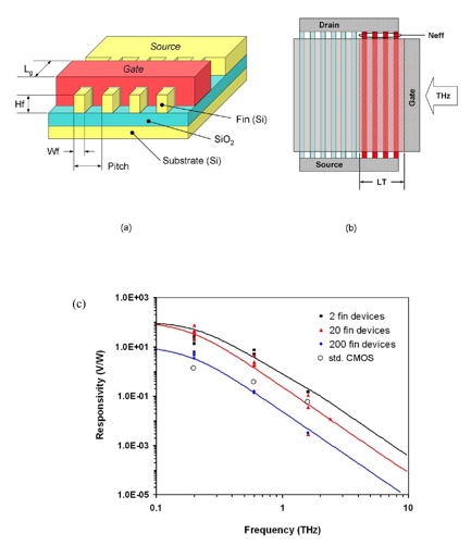
Figure 1 (a) Schematic illustration of FIN FET (field effect transistor) device structure (the drain region is omitted from the foreground for clarity). The vertical channel fins are surrounded by the gate dielectric and gate conductor forming an effective dual gate MOSFET (metal-oxide-semiconductor field-effect transistor). (b) Conceptual illustration of the effective number of fins (in red) in a given device contributing to response. Fins beyond the characteristic transfer length LT behave as a load to the response. © Open drain responsivity of several FIN FET devices at various incident frequencies. Filled symbols are measured data; lines are modeled response. Device gate length is 100 nm. Open symbols are measured responsivity for standard CMOS FETs.
Credits: Dmitry Veksler, Bill Stillman, Chris Donais and Michael Shur
